This PLECS demo model analyzes the performance of Type 2 and Type 3 analog compensators used in power supply units (PSUs). The analyzed PSU is a buck converter with modeled-in inductor and capacitor non-idealities. The role of the capacitor and its effective series resistance (ESR) on the plant zero and poles is discussed. Furthermore, the compensators' performance is analyzed with respect to the phase margin, system bandwidth, and rate of change in gain at the crossover frequency.
Power Circuit
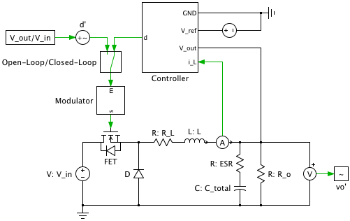
The analyzed PSU is a simple buck converter where the capacitance and ESR effects are being investigated. The plant transfer function can be simplified to the following:

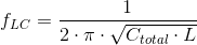
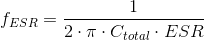
where the Laplace operator, 's', and thus the plant transfer function, varies as a function of the frequency. In GPlant(s), the effects of the inductor resistance are assumed to be minimal on system performance and, thus, ignored. For the buck converter, the system double poles and zero due to the LC-filter and ESR, respectively, are given by:
The voltage controllers are designed to obtain desired open-loop system characteristics by placing the system poles and zeros.
Controls
The model can be run either as an open-loop or closed-loop controlled system. Double-clicking on the Manual Switch ("Open-Loop/Closed-Loop") toggles the model configuration. The closed-loop control system consists of a voltage-mode regulator and over-current protection. The voltage-mode regulator can be configured to operate either with a Type 2 or Type 3 compensator.
The closed-loop system should have the following characteristics to ensure high system dynamics and stability:
- A system bandwidth between 1⁄10 and 1⁄5 of the switching frequency.
- A -20 dB/decade slope of the gain near the system crossover frequency.
- A phase margin greater than 45°.
Type 2 Compensator
Type 2 compensators are used in systems where the desired crossover frequency (fx) is greater than both fLC and fESR. That is:
fLC < fESR < fx < fsw/2,
where fsw/2 is half the switching frequency. We will refer to this as System 1.

The Type 2 compensator in the model shown above is implemented using an ideal op-amp with finite gain. The op-amp gain is set to 106. The positive input terminal is connected to the reference voltage. The output voltage of the buck converter is scaled using a resistive divider and connected to the negative input terminal of the op-amp. Furthermore, the negative input is connected to the op-amp output via an RC network.
The simplified transfer function of the Type 2 compensator is given by:
To obtain the desired system performance, the resistors and capacitors can be selected to ensure that the zero and poles meet the following requirements:
fz1 ≈ 0.75 · fLC
fp2 ≈ fsw/2
Placing the zero and pole at these locations, along with the pole at the origin (fp1), causes the open-loop transfer function of the closed-loop system to exhibit the desired characteristics.
Type 3 Compensator
In systems where fx is less than fESR, the Type 2 compensator may not be able to provide the desired closed-loop system response and stability. A Type 3 compensator can then be used.

As with the Type 2 compensator, the Type 3 compensator is implemented with an ideal, finite-gain op-amp. The Type 3 compensator configuration is shown above. For systems where:
fLC < fx < fESR < fsw/2,
the additional pole and zero of the Type 3 compensator allow for the design of a fast and stable closed-loop control of this system. We will refer to this as System 2.
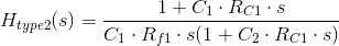
The simplified transfer function of the Type 3 compensator is given by:

To obtain the desired system performance, the resistors and capacitors can be selected to ensure that the zero and poles meet the following requirements:
fz1 ≈ 0.75 · fLC
fz2 ≈ fLC
fp2 ≈ fESR
fp3 ≈ fsw/2
Placing the zeros and poles at these locations, along with the pole at the origin (fp1) causes the open-loop transfer function of the closed-loop system to demonstrate the desired characteristics.
Overcurrent Protection
An IR3840 synchronous buck regulator based over current protection is modeled in this circuit. This is used to limit the current that is drawn from the input voltage source. As the current through the inductor reaches the maximum allowable current in the system, the switching modulation index is set to 0. After a few clock cycles the over current protection system is reset.
Simulation
The model has been configured to emulate the two different systems described above. In the compensator design process, the open-loop plant transfer function is used to verify the analytical model of the plant. Using the PLECS Analysis Tools, the frequency response of both the unregulated and closed-loop controlled converter can be generated. The resulting Bode plots can then be used to determine if the system bandwidth, crossover frequency, gain and phase margins requirements are met.
Try it
This model is available in the PLECS Demo Model library provided in both versions of PLECS.